AMO, CNST and RWTH develop monolithically integrated CMOS compatible perovskite lasers with record low thresholds
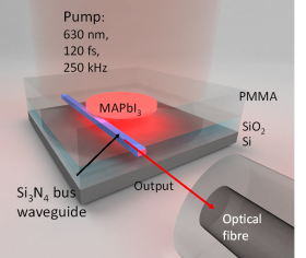
Researchers of AMO GmbH and RWTH Aachen University together with colleagues from Center for Nanoscience and Technology (a division of Italian Institute of Technology) have recently developed perovskite microdisc lasers integrated into silicon nitride photonic circuits. This optically pumped lasers have thresholds of 4.7 µJcm-2 surpassing the thresholds of other CMOS compatible lasers. These results were published in Nano Letters (DOI: 10.1021/acs.nanolett.8b02811).
Our lasers are based on solution processed direct band-gap semiconductors – metal-halide perovskites. Unlike III-V alloys, which are used in the established devices, perovskites can be obtained by spin-coating and annealing at low temperatures on arbitrary substrates. In a stark contrast to III-Vs, which suffer from the high non-radiative recombination losses if not grown on matching substrates by high-temperature processes, such perovskite layers exhibit a high optical gain. This makes this material suitable for monolithic integration of optoelectronic devices on silicon substrates, which will result in a substantial reduction of the cost of integrated photonic systems, which are mostly driven by the assembly of external laser sources.
Perovskites, however, due to their high chemical sensitivity are incompatible with standard semiconductor fabrication processes, which, until now, held back the further development of integrated perovskite optoelectronic devices. At AMO we have solved this problem by developing the first truly scalable fabrication process based on optical lithography.
The research has been funded by the European Union’s Horizon 2020 research and innovation programme under the Marie Sklodowska-Curie grant agreement no. 643238 (Synchronics) and PPP no. 688166 (Plasmofab).