HIPER-LASE: Towards perovskites lasers for silicon photonics
The DFG-funded project HIPER-LASE has kicked-off on October 5, 2021, to explore the potential of perovskite semiconductors for realizing an on-chip electrically pumped laser.

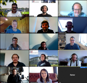
A (virtual) group picture taken during the kick-off meeting of the project hyper-lase.
Integrated photonic-circuits could trigger the next technological revolution in microelectronics. The prerequisite, however, is the availability of a cost-effective and scalable manufacturing technology. An excellent candidate for this task is the photonics platform based on silicon/silicon-nitride. What is still missing though, is an integrable laser source. In the DFG-funded project HIPER-LASE, AMO and partners RWTH Aachen University, the University of Wuppertal and the University of Siegen will explore the potential of perovskite semiconductors for realizing an on-chip electrically pumped laser. The project had its kick-off meeting on October 5, 2021.
“Metal-halide perovskite semiconductors are wonderful materials, full of interesting properties”, says Dr. Piotr Cegielski, senior researcher at AMO GmbH. “They have already proven very successful for fabricating solar cells and LEDs. One of their main advantages is that they can be fabricated from solution processes, which makes them compatible with silicon technology. At AMO, we have already demonstrated the first on-chip optically pumped-perovskite laser. What remains to be understood is if it is possible to realize also an electrically pumped laser and/or to achieve continuous wave operation. And this is the ambitious goal of the project HIPER-LASE.”
Indeed, HIPER-LASE will explore the fundamental limits of metal-halide perovskites as electrically-pumped gain media. This requires answering questions that have remained largely unaddressed in the context of perovskite solar cell research, such as understanding loss mechanisms and charge carriers dynamics under high excitation, identifying suitable electrical contacts for high current densities, and developing appropriate concepts for heat management.
To address these questions, HIPER-LASE brings together the complementary expertize of four different groups: the nanophotonic group led by Laser physicist Dr. Anna Lena Giesecke at AMO, with extensive know-how in fabrication and characterization of nanophotonic devices and perovskite micro-lasers; the group of Prof. Thomas Riedl at the University of Wuppertal, which has wide-ranging experience in the physics and technology of semiconductor lasers and of perovskite processing; the group of Prof. Max Lemme at RWTH Aachen University, with expertise in semiconductor fabrication-technology and characterization of opto-electronic devices; and finally the group of Peter Haring Bolívar at the University of Siegen, with 25 years of experience in nanoscopic optical pump-probe and THz analysis of materials and devices.
The partners will identify to what extent the morphological, optical, electrical and thermal properties of perovskites can be optimized towards electrically pumped lasing using the broad range of methods available in the consortium. “At the end of the project we want to be in a position to understand, based on rigorous scientific evidence, whether metal-halide perovskites can deliver on-chip electrically-driven lasers, and what is needed to realize them”, says Prof. Max Lemme. “In a sense, we are doing the necessary homework for setting the basis of a technology that, if successful, will be a real breakthrough in the field of integrated photonic circuits, with major implications for several applications – including high-speed data communication, food quality monitoring and medical sensors.”
HIPER-LASE is a project funded by the German Research Foundation (DFG) – Project number 441341044.


