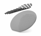
A scalable method for the large-area integration of 2D materials
Two-dimensional (2D) materials have a huge potential for providing devices with much smaller size and extended functionalities with respect to what can be achieved with today’s silicon technologies. But to exploit this potential we must be able to integrate 2D materials into semiconductor manufacturing lines – a notoriously difficult step. A team of researchers from […]