Technology Transfer

From lab to innovation

AMO’s misison is to build a bridge between academic and industrial research. We make the results of our research work available to industry, high-tech start-ups and other external partners. We build on the know-how gained in publicly funded projects to develop tailored solutions for our customers, responding flexibly to their needs. We also do contract research and support innovative spin-offs. In this way, we pave the way for innovation. The basis of our activities — be it research, consulting or prototype development —  is our fully equipped clean room, which is open to all partnerships.

Let us talk

How may we help you?

AMO is organized to find the best possible individual solution for all customers and partners.

  • Are you looking for innovative solutions to improve your products or processes? We offer customized approaches based on our research results.
  • Do you have a tech-based business idea and want to start a new company? We offer you research and development expertise to develop innovative solutions and to create a spin-off company. We accompany you from concept phase to market launch.
  • Do you need a dedicated solution for a specific research theme? You can outsource your research to us and we’ll work closely with you to develop customized solutions.
  • Do you need a cleanroom environment for your research and development? We offer you the possibility to develop your individual solutions in our cleanroom.

Let us talk about your needs and ideas.

Contact

Dipl.-Ing. Herbert Kleinjans

Head of Services, Operations & Communications (COO)


Product and services

An overview of the products and services available to our customers and partners.

Nanostructuring

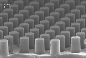
AMO offers a highly flexible process-platform for the fabrication of nanostructures. We have a broad range of lithography techniques that can be flexibly combined with each other – including interference lithography. Each lithography technique is tailored to a specific pattern-transfer process and can be used on a wide range of substrates. In addition, we have developed an advanced nanoimprint lithography process that can transfer e-beam-defined patterns to large areas in a cost-effective manner.

Lithography

AMO offers a range of lithographic tools, including

  • Optical lithography
  • Interference lithography
  • Electron beam lithography

Each of these lithographic techniques is specifically tailored to the ensuing patterning process and can be used on a variety of substrates, from conventional silicon wafers to glass substrates and flexible substrate films. The lithography technique used depends mainly on the required minimum structure-size and other specific parameters of the device.

For more information on the different lithography technologies or for specific advice for your application, please do not hesitate to contact us.

Download

Nanoimprint

Nanoimprint is a precise molding technology in which a stamp with a 3D structure is brought into direct contact with a UV-curable resist on a substrate.  Thanks to the low viscosity of the resist, the structures on the stamp fill within seconds by applying a small pressure, and are then hardened by UV light. After the curing process, the substrate with the imaged structures can serve as a functional layer, or the structures can be transferred into the substrate itself using RIE process.

We offer our customers a commercially available UV-curable resist – AMONIL® and a suitable adhesion promoter – AMOPRIME. In addition, we have extensive know-how in the production of master stamps for nanoimprint applications. Thanks to the many years of experience in this field and the wide range of lithographic processes available in our clean room, we can offer our customers high-quality and precise solutions for their specific requirements.

AMO has developed a commercially available UV-curable resist (AMONIL®) and a suitable adhesion promoter (AMOPRIME). The resist AMONIL® is characterized by excellent profile accuracy, outstanding coating and imprint properties, and sufficient plasma stability.

Application

  • UV-based nanoimprint lithography

Properties

  • Can be used with standard spin coating
  • Suitable for quartz, PDMS and PFPE molds
  • Good adhesion to silicon substrates
  • AMONIL® adheres well to different substrates such as SiO2, Ti, Au and PE. The adhesion can be improved by using AMOPRIME.
  • The use of AMOPRIME enables also imprint on GaAs, GaN, InP, Al2O3

Specifications

  • Viscosity of the base material: 50mPa s
  • Photoactivator designed for UV annealing
  • Proven capacity for Step&Repeat cycles > 1000 imprints
  • Required dose: 2J/cm² when using a quartz mold

Availability:

  • AMONIL available in 3 variations with film thicknesses from100 to 800 nm
  • AMOPRIME available as adhesion promoter

For further details please refer to the FactSheet.

Interference Lithography

Interference lithography (IL) is an optical lithography technique based on holographic principles. In this process, an interference pattern formed by two ultraviolet light beams is transferred into a high-resolution, light-sensitive resist. The resulting patterns are stitching-free and spatially coherent over many square centimeters, and allow realizing structures smaller than 100 nm.

Thanks to its precision, IL technology is particularly well suited for the production of:

  • large-area gratings
  • periodic nanostructures
  • porous surfaces
  • photonic crystals

In addition, interference lithography is also used for realizing optical components, masters for nanoimprint and micro-optics, and to create biocompatible surfaces. Furthermore, it is of great relevange for the production of precision measurement tools.

Our expertise

The IL process at AMO is specifically designed for high contrast gratings. Two actively-stabilized interferometers are available for this purpose.  We offer flexible exposure and development services for gratings. Structure transfer and further processing are carried out according to individual customer requirements. Different substrate sizes are available. Our process enables anisotropic pattern-transfer. All dimensions of the grating are specified and controlled during and after processing. Line Mapping and Line Edge Roughness (LER) characterization are available upon request.

Further specifications in the Fact-Sheet.

Download

Prototyping

Our offering includes research expertise and prototyping services in the field of micro- and nanotechnology, for applications in electronics, photonics, sensor technology and biotechnology, among others. Our flexible R&D infrastructure enables us to meet cross-industry specifications and provide tailored solutions for our customers.

Our technology platform includes:

  • Si and SiN nanophotonics
  • Graphene foundry services
  • Nanostructuring

In addition, we offer the following services:

  • Electron beam lithography (CD ~10nm)
  • Optical lithography (CD ~500nm)
  • Interference lithography
  • Nanoimprint technology
  • Structure transfer
  • Different deposition processes

Our strengths:

  • Customized services, from proof-of-principle demonstrations to small-scale production
  • Flexible integration of new materials and technologies
  • Short turnaround times thanks to effective process control and an experienced team
  • Optimization of processes from concept development to finished demonstrator
  • Protection of customers’ intellectual property (IP Protection)

The close feedback loop with our customers allows us to develop solutions tailored to the customer’s specific needs.

Download

Graphene Devices

AMO offers its customers the opportunity to fabricate graphene devices according to their specific needs. Customers can choose between single wafers tailored to their specific requirements and multi-project wafers offered as part of the 2D EPL project. The devices include back-gated, top-gated and dual-gated transistors that enable sensing applications (e.g. Hall sensors, biosensors, etc.). It is also possible to fabricate integrated circuits such as graphene integrated MMICs.

As part of its graphene foundry services, AMO also supports customers in developing their own processes. Detailed capabilities and applications can be discussed in one-to-one meetings. Below are some technology key points.

Technological basis

Substrate

  • Size 1×1 cm up to 8″
  • Glass
  • Silicon
  • SOI
  • Flexible substrates

Structuring / Lithography

  • Resolution up to 100 nm
  • Up to 4-layer lithography
  • Etching (wet & dry)
  • Lift-off processes

Deposition

  • Different CVD systems (SiO2, Si3N4, graphene, …)
  • ALD (Al2O3, TiO2, AlN, TaN, TiN)
  • Sputtering (Cu, Ni, …)
  • Evaporation (Al, Ni, Au, Pd, Ti, Cr)
  • In-house wet transfer of graphene

Characterization

  • Electrical measurements (DC, RF)
  • Raman spectroscopy
  • Ellipsometer measurements
  • Electron microscopy
  • Optical microscopy
Graphene-based flexible Hall sensor

Download

Active and passive photonic components

AMO offers research and development services as well as low-volume production of silicon and silicon nitride nanophotonic devices and circuits. AMO’s process-line includes a wide range of processes from single silicon/silicon nitride passive nanophotonic chips to 6” wafers with active nanophotonic devices and two metal layers.

Currently we offer commercially the following components and processes:

Passive components

  • Processes for strip, ridge, slotted waveguides and combined waveguide technology
  • Low-loss waveguides
  • Resonators
  • Fiber-chip coupling

Active components

  • Processes for n+ and p+ doping and metal interconnects as well as processes for integrated titanium-based microheaters
  • Heaters
  • Modulators
  • IR detectors

Download

Metrology Services

AMO’s research infrastructure includes a wide range of analytical tools for metrological studies on small substrates as well as up to 6” wafers.

Currently, we offer the following measurement services:

  • Optical properties of thin films and transparent substrates
  • Surface morphology
  • Surface texture
  • Raman and photoluminescene measurements
  • Dimension measurements like film thickness
  • Electrical measurements
  • Resistivity measurements

Analytical characterization techniques

  • Scanning probe microscopy
  • Ellipsometry
  • Dektak surface profiler
  • Raman spectroscopy
  • Scanning electron microscopy
  • Terahertz spectroscopy (in cooperation with Protemics)

Electrical characterization tools

  • Parameter analyzers
  • Probe station
  • Impedance analyzer
  • Agilent pA-meter and Agilent Precision
  • LCR mater

Photonic devices characterization

  • @1300 nm and 1550 nm
  • Tunable laser
  • Butt and fiber coupled

More information on the individual tools can be found here.

Contact

Dr. Satender Kataria

Group Leader - Metrology