
Successful finalization of the FP7 European Project “PLATON”: Merging Plasmonics and Silicon Photonics
With the final actions in March 2015, a successful conclusion of the European research project PLATON targeting the integration of Plasmonics and Silicon Photonics has been achieved. The aim of the PLATON project was the realization of a new class of optical interconnects for the application in backplanes and Blade Servers, employing Plasmonics as a disruptive technology to achieve Terabit per second optical routing.
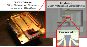
Final PLATON-Router chip, merging Plasmonics and Silicon Photonics on one SOI platform.
Coordinated by the Greek C entre for Research and Technology Hellas all projects partners, Fraunhofer Gesellschaft Institut fuer Zuverlaessigkeit & Mikrointegration in Berlin, the Syddansk Universitet Denmark, Universite de Bourgogne France, the Institute of Communication and Computer Systems Greece and AMO GmbH, Aachen, worked in close collaboration to address the challenging project tasks. Within the PLATON project a Router-chip with integrated nanophotonic, plasmonic and microelectronic components has been successfully realized (see figure). A comprehensive technology toolkit for the realization of the SOI platform and the integration of plasmonic structures has been developed. The SOI platform, manufactured by AMO, consists of all silicon nanophotonic and microelectronic devices and provides a cavity as an interface for the integration of the plasmonic devices, which are realized by an innovative contact lithograhpy process developed by Universite de Bourgogne .
Two different 8×1 MUX/DEMUX structures fabricated on the SOI platform for multiplexing two different incoming DWDM streams have been successfully demonstrated[1], performing at two different wavelength bands and enabling in this way their use along with a 2×2 switch in chip-scale routing applications. These dual-stream MUX/DEMUX elements operate for eight 100GHz-spaced channels per stream offering at the same time a 40GHz 3-dB bandwidth and yielding a record performance of 40% in terms of the high-bandwidth versus channel density ratio.
On the same SOI platform, an ultra-compact and low-power thermo-optic (TO) silicon-plasmonic 2×2 MZI structure for data switching applications has also been demonstrated[2]. By using the novel material “Cyclomer” a successful reduction of the footprint has been achieved, resulting in the smallest footprint among plasmonic MZI TO switches reported so far. As a result of the reduced length of the plasmonic sections, the Cyclomer-loaded plasmonic MZI switch exhibited improved efficiency (power consumption × response time × active length). The enhanced potential compared to plasmonic switches based on other material systems was documented by NRZ data analysis. The Cyclomer-based plasmonic switch was evaluated with 10Gb/s NRZ data traffic for both ON and OFF switching states, resulting in successful switching operation without significant signal degradation.
These results represent a substantial contribution for further steps towards enabling high-throughput, low-energy and fast routing circuitry within the same photonic Network-on-Chip (NoC), utilizing the silicon 8×1 MUX elements as the front-end of the NoC and cascading the compact and low-power Cyclomer-based plasmonic 2×2 TO switch at their output.
[1] S. Papaioannou, D. Fitsios, G. Dabos, K. Vyrsokinos, G. Giannoulis, A. Prinzen, C. Porschatis, M. Waldow, D. Apostolopoulos, H. Avramopoulos, and N. Pleros, “On-Chip Dual-Stream DWDM 8-Channel-Capable SOI-Based MUXs/DEMUXs with 40 GHz Channel Bandwidth”, IEEE Photonics Journal, Vol. 7, No.1, 7900210, February 2015 (DOI: 10.1109/JPHOT.2014.2381639).
[2] S. Papaioannou, G. Giannoulis, K. Vyrsokinos, F. Leroy, F. Zacharatos, L. Markey, J.-C. Weeber, A. Dereux, S. I. Bozhevolnyi, A. Prinzen, D. Apostolopoulos, H. Avramopoulos, and N. Pleros, “Ultra-Compact and Low-Power Plasmonic MZI Switch Using Cyclomer Loading”, accepted for publication in IEEE Photonics Technology Letters, February 2015 (DOI: 10.1109/LPT.2015.2404942).
Acknowledgements: European FP7 ICT projects PLATON and PHOXTROT under Contract 249135 and Contract 318240, respectively.
Please find the complete press release here: