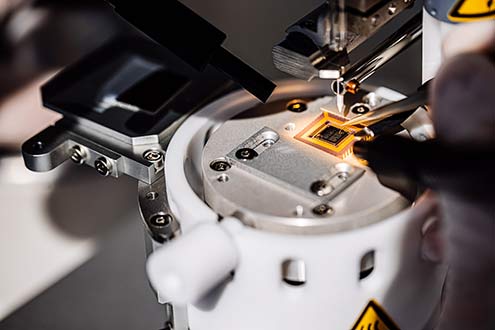
AMO and RWTH recently developed an experimental method for proper visualization of graphene grain boundaries
Researchers of AMO GmbH and RWTH Aachen University as well as their colleagues developed an experimental method for proper visualization of graphene grain boundaries. The work was conducted in collaboration between AMO GmbH, RWTH Aachen University, the Royal Institute of Technology (KTH) Stockholm and Chemnitz University of Technology.
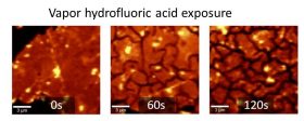
This method for evaluating atomic-scale defects in graphene could help to boost large scale production of the ‘wonder’ conductor. Results of these research activities have recently been published in Science Advances entitled “Direct observation of grain boundary-based line defects in graphene with optical microscopy and scanning electron microscopy after vapor hydrofluoric acid exposure”.
The study provides a method to simply, quickly and cost-effectively observe the size and distribution of grain boundaries on a large scale by using standard processes in wafer fabs, namely vapor hydrofluoric acid (VHF) etching and optical microscope inspection. In terms of simplicity, speed and scale, there exists no comparable method for visualizing grain boundaries in large-area CVD graphene on silicon dioxide (SiO2) substrates. Large improvements to macroscopic material properties are expected by enabling controlled process engineering of these unavoidable defects.”
 The research was funded by the European Research Council through the Starting Grants M&M’s (277879) and InteGraDe (307311), the Swedish Research Council (GEMS, 2015-05112), the China Scholarship Council (CSC), the German Federal Ministry for Education and Research (NanoGraM, BMBF, 03XP0006C), the German Research Foundation (DFG, LE 2440/1-2) and the German Research Council (DFG) through the Priority Program SPP 1459 Graphene.